Integrated, high-performance optical solutions for the industry
CEA-Leti's photonic platform is developing next-generation optical components and systems for telecommunications, cybersecurity, health, and augmented reality. It relies on unique equipment in Europe and includes 300 researchers.
With a portfolio of 700 patents, the platform is at the forefront of European optical and photonic innovation. It covers every aspect of their development: device design, semiconductor technologies, component manufacturing, system integration, packaging, and small series for sampling.
Researchers are in charge of developing manufacturing processes for every optical material (III-V, II-VI, silicon, etc.), with wafer sizes ranging from 2 inches to 300 mm. The platform adjoins industrial facilities where manufacturing processes are validated, supporting the transfer of innovative and competitive solutions to the industry.
|
What expertise do industrial partners receive?
• Increased miniaturization of components and features • Reduction of optical losses and power consumption
• Integration of silicon with III-V or II-VI materials • Quantum photonics for high-performance computing and secure communications • Manufacturing processes for photonics • Eco-innovation
|
|
Cutting edge preindustrial equipment
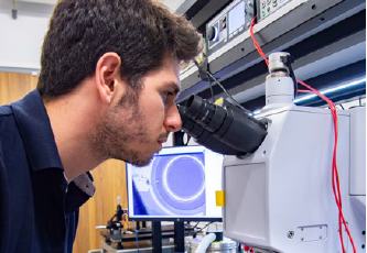
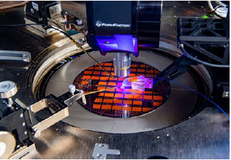
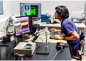
• Wafer-level collective optical characterization benches using probe testing
• Photonics dedicated packaging and assembly equipment developed in partnership with equipment manufacturers: high-precision fiber-optic alignment, image sensors bonding, etc.
• CEA-Leti works with CEA Tech Nouvelle Aquitaine’s PIMS platform, using optical test and characterization means
|
|
How to work with
the photonic platform?
CEA-Leti’s teams support the innovation needs of industrial partners throughout all development stages via bilateral contracts or common laboratories. The platform has approximately thirty partners, such as startups, small and medium-sized companies, or major French and international groups in various fields. A few example: Lynred (cooled and uncooled infrared vision), Trixell (medical imaging), Aledia (displays), Microoled (microdisplays), III-V Lab, etc.
|