Advanced materials: a driver of opportunities
New materials underpin innovation in emerging fields such as IoT, automotive engineering, energy, health monitoring and micro and nano electronics.
Leti's expertise in epitaxy is a continuous source of innovative devices: GaN-on-Si 200 mm for power devices [1], GaN-on-SiC or sapphire for LEDs [9, 10], GeSn for lasers, Ge for photonics [2], CdHgTe for infrared detectors [8]. Development of 2D materials such as MoS is in progress using innovative processes [3].
Leti is a pioneer in wafer bonding: SOI, FDSOI, Coolcube technologies, first 300 mm InGaAs-on-insulator substrates for upcoming microelectronics nodes [4] and 3D integration [5] based on direct bonding. New generations of dedicated substrates are currently under study.
Leti is closely involved in thin film deposition including Lead Zirconate Titanate for MEM tunable filters and memories [6]. It is also a key player in the latest generations of dielectrics, interconnects, chalcogenides, polymers, electrolytes, electrodes and packaging materials for nano electronics, nano energy sources and nano biotechnologies.
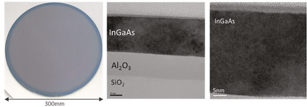
Left: Picture of an InGaAsOI substrate after layer transfer.
Right: TEM and HR-TEM images of the transferred InGaAs layer on Al2O3 buried oxide.
Referenced publications in annual research report 2015:
[1] L. Di Cioccio, E. Morvan, M. Charles, et al. “From Epitaxy to Converters Topologies what Issues for 200 mm GaN/Si,” 2015 IEEE International Electron
Devices Meeting (IEDM 2015), 07 Dec - 09 Dec 2015, Washington, DC, USA.
[2] Y. Bogumilowicz, J.M. Hartmann, R. Cipro, R. Alcotte, et al. "Anti-phase
boundaries–Free GaAs epilayers on "quasi-nominal" Ge-buffered silicon substrates", , Appl. Phys.
Lettboundaries–Free GaAs epilayers on "quasi-nominal" Ge-buffered silicon substrates", , Appl. Phys. Lett. 107, 212105 (2015).. 107, 212105 (2015).
[3] S. Cadot, F. Martin, O. Renault, M. Fregnaux, D. Rouchon, E. Nolot, L.Veyre, C. Thieuleux, E. A. i;
“Low-temperature Atomic Layer Deposition of MoS2 using a novel organometallic precursor”, Extended Abstract of the 15th International Conference on Atomic Layer Deposition, 29th June-1st July 2015
[4] J. Widiez, S. Sollier, T. Baron, M. Martin, et al. "First demonstration of 300 mm InGaAs-On-Insulator substrates fabricated using the Smart Cut™ technology", Proceedings of SSDM conference, 2015
[5] L. Benaissa, L. Di Cioccio, Y. Beilliard, P. Coudrain et al., "Next Generation Image Sensor via Direct Hybrid Bonding", Proceeding of EPTC 2015.
[6] I. Gueye, G. Le Rhun, P. Gergaud, O. Renault, et al. "Chemistry of surface nanostructures in lead precursor-richPbZr0.52Ti0.48O3 sol-gel films", Applied Surface Science, Vol. 363, pp. 21-28, 2015.
[7] G Laval et Al, Inter. Conference on Nitride Semiconductors (ICNS 2015)
[8] C.Thomas, X.Baudry, s, M.Veillerot, P.H.Jouneau, S.Pouget, O. Crauste, T.Meunier, L.P.Lévy, P.Ballet, J. Cryst. Growth 425, 195 (2015). hgte
9] Piero Gamarra, Cédric m, Maurice Tordjman, François Templier and Marie-Antoinette di Forte-Poisson, "Dual wavelengths InGaN/GaN MQW and LED structures", 16th European Workshop on Metalorganic Vapour Phase Epitaxy (EWMOVPE XVI), June 7 – 10, 2015, Lund, Sweden
[10] A. Dussaigne, P. Ferret, R. Obrecht, M. Lafossas, A. Coquiard, A. Fargeix, R. Caulmiloné, P. Guénard and F. Lévy, III-N MOVPE overgrowth, material quality and LED structures on GaNoS and GaNoMo advanced substrates, Proceeding Inter. Conference on Nitride Semiconductors (ICNS 2015) ganos.