- Digital speed performance without any sacrifice
The integration of digitalisation in people’s everyday lives has opened the floor to new opportunities for innovation in several sectors. A digitalised world plays an important role not only in economic growth and job creation but also in accelerating access to knowledge and education. Such technological advancement requires sufficient hardware systems.
Responding to the need for digital transition in the mobile and IoT industry, CEA-Leti, a CEA technology research institute, together with SOITEC developed a patented Smart CutTM process to manufacture substrates to produce digital and low power consumption electronic components. With this groundbreaking process, higher data speed, longer battery life, digital processing and power management integration can be achieved, meeting the demanding market’s request.
- Upscaling data speed standards
Nowadays, each connected object contains several semiconductor components for data reception, computing, sensing, system management, as well as data emission. Radio
Frequency Front End Modules (RF FEM), the key elements to move to 4G+, 5G and future 6G standards, enable signal reception and transmission. However, they require high performance in terms of computing and energy power consumption at the same time. To respond to the needs of RF applications to improve the speed, quality and high computing capabilities of smartphones, a generic fabrication process named Smart Cut™, invented by CEA-Leti in 1994, has been used by SOITEC to develop RFSilicon-on-Insulator (SOI).
- Giving birth to new products
CEA-Leti, in collaboration with SOITEC, have created the patented Smart Cut™ process of substrate fabrication, which consists of various technological steps such as oxidation, implantation, cleaning before bonding. Smart Cut™ results in a transfer of a thin active layer of silicon from one substrate to another, which can be used in all electronic devices. This process provides different family of products: the main one is dedicated to RF components for reaching high performances and power optimization for smartphones. In addition, another main technology, named FDSOI, is a key technology well suited to mixed analogue/ radio frequency and digital circuits, allowing Europe to create advanced microprocessor manufacturing capacity with STMicroelectronics and GlobalFoundries. Based on Smart Cut™, the REFERENCE project is developed to improve SOI substrates for mobile communications, scaling up a pilot line from 200mm to 300mm substrates.
- Endless opportunities in many manufacturing processes
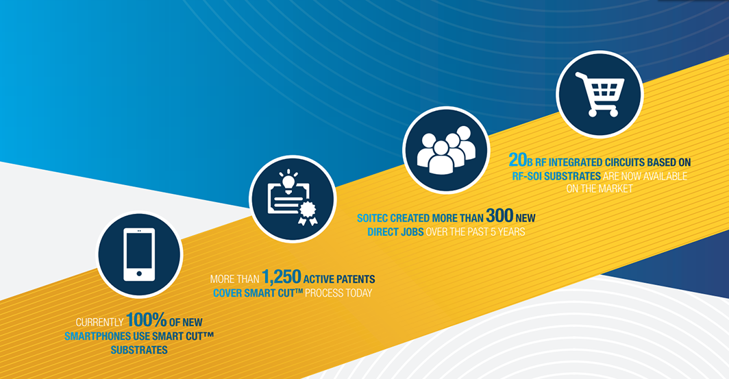
CEA-Leti and SOITEC new SOI substrates have met immediate commercial success worldwide, where 100% of new smartphones integrate these substrates. Over the past 5 years, SOITEC has gained €1B thanks to the 300mm process and created more than 800 permanent jobs. SOITEC’s has many world leading clients, including STMicroelectronics, Samsung, GlobalFoundries and SONY. Today, about 20B RF integrated circuits based on RF-SOI substrates are available on the market. Such substrates allow an efficient power reduction enabling a longer battery life, without sacrificing digital speed performance as well as providing a good balance between digital performance, mixed signal compatibility, power consumption and cost.