Addressing the challenges of semiconductor spin qubits
Published on 8 February 2024
Body text 2
- To implement its solid silicon-based technology expertise in the quantum sphere, CEA-Leti has, as of January 2021, a diversely skilled team of more than 50 people working on quantum development, with a large portion holding doctorates and post-doctoral qualifications.
- Expertise includes micro- and nanoelectronics; simulation and modeling; 2D and 3D materials; device architecture and design (including both logic and memory); mask development; 3D integration and packaging; integrated circuits; physical characterization (in-line and off-line); electrical characterization and reliability; the emerging field of ultralow temperature cryo-CMOS; and software. These skills are complemented by CEA-IRIG and CNRS who are experts in quantum engineering, physics of scaled nanostructures, quantum physics.
CEA-Leti, CEA-IRIG, and CNRS share more than 7 cryogenics equipements as well as operation expenditures in the silicon platform and capital expenditure include the acquisition of a novel cryogenic wafer prober (from the leading cryogenic company Bluefors) for automatic measurements of 300mm wafers down to temperatures of 2K.
How does the CEA-Leti organization intend to apply these intellectual and physical resources to create qubits using silicon?
- From a strategic perspective, it’s important to keep in mind that, in principle, silicon-spin represents perhaps the simplest path towards implementation of a two-level quantum system. A powerful example of this potential came with the ISSCC 2020 publication, which described the 28nm FD-SOI Quantum Integrated Circuit (QIC) developed by CEA-Leti, CNRS and CEA-Irig through Quantum Silicon Grenoble. The device represents the first demonstration of integrating conventional electronic devices and elements with quantum dots on a CMOS chip, combining crucial analog and digital instrumentation with quantum structures fabricated on the same semiconductor layer.
- As the ISSCC paper stated, "the quantum silicon choice allows the IC community to integrate large-scale qubit-control electronics directly [adjacent to] the quantum silicon core, thus drastically reducing the wire-connection number and qubit-addressing fanout, meanwhile increasing the operation bandwidth for error correction and the spin-readout sensitivity."
Loïck Le Guevel, a lead author on the paper and member of the Quantum Silicon Grenoble research group led by Maud Vinet, noted that the device "uses all elements required to properly design high-spec state-of-the-art circuits, such as passive elements, resistors and capacitors, transistors for digital operation up to 7Ghz, and transistors for analog operation up to 3Ghz. On top of that, we were able to design a double quantum dot in the same semiconductor layer as transistors using a standard fabrication flow. This realization emphasizes that FD-SOI could one day allow circuit designers to use qubit arrays embedded in IP blocks with classic electronics to build custom-made, large-scale quantum silicon processors.
| 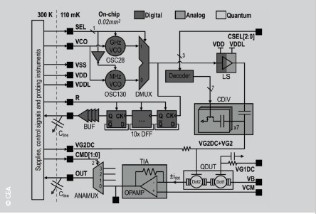
QUANTUM CIRCUIT Functional block diagram of the mixed digital-analog signal circuitry interfacing a quantum device at 110mk
|
Top page